Part 17: Detailed Circuit-Level Design of Image-Based Scanner Systems (Power, Sensor, Processing, and Interface Integration) |
1. Introduction to Circuit-Level Design |
1. The circuit-level design of an image-based scanner is where optics, electronics, and embedded computing converge into a single functional system. |
2. Unlike high-level architecture, circuit design focuses on: |
* Electrical signal integrity |
* Power regulation and distribution |
* Sensor interfacing |
* High-speed data routing |
* Noise suppression |
* Real-time processing support |
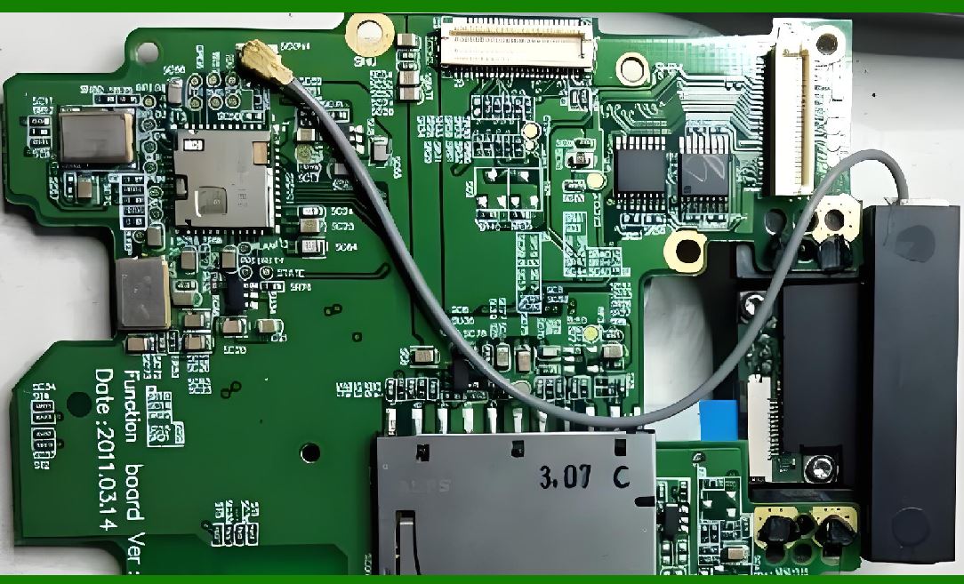
3. A modern scanner PCB is essentially a mixed-signal embedded vision platform. |
|
2. System-Level Circuit Partitioning |
2.1 Major Circuit Domains |
1. Power management circuit |
2. Image sensor front-end circuit |
3. Processing subsystem circuit |
4. Memory subsystem circuit |
5. Communication interface circuit |
6. Illumination driver circuit |
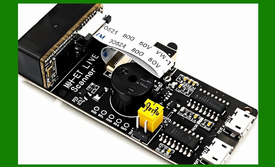
2.2 Signal Domain Separation |
1. Analog domain: |
* Sensor outputs |
* Analog front-end |
2. Digital domain: |
* CPU/SoC processing |
* Communication interfaces |
3. Power domain: |
* Voltage regulation |
* Current distribution |
|
3. Power Supply Circuit Design |
3.1 Input Protection Circuit |
1. Includes: |
* ESD protection diodes |
* Surge suppression components |
* Reverse polarity protection |
3.2 DC-DC Conversion Stage |
1. Converts input voltage (e.g., 5V USB or battery voltage) into required rails: |
* Core voltage (1.0V.2V) |
* IO voltage (1.8V.3V) |
* LED driver voltage |
3.3 Low-Dropout Regulators (LDOs) |
1. Used for: |
* Noise-sensitive analog circuits |
* Image sensor power supply |
3.4 Power Sequencing Circuit |
1. Ensures correct startup order: |
* Core logic first |
* Sensor and peripherals later |

|
4. Image Sensor Interface Circuit |
4.1 CMOS Sensor Connection |
1. Typical interfaces: |
* MIPI CSI-2 |
* Parallel bus (legacy systems) |
4.2 High-Speed Signal Routing |
1. Requirements: |
* Controlled impedance traces |
* Differential pair routing |
* Length matching |
4.3 Clock Generation Circuit |
1. Includes: |
* Crystal oscillator |
* PLL (Phase-Locked Loop) support |
4.4 Sensor Power Conditioning |
1. Multiple regulated rails: |
* Analog sensor supply |
* Digital sensor supply |

|
5. Image Signal Processing Circuit |
5.1 ISP Integration |
1. Functions: |
* Demosaicing |
* Noise reduction |
* Color correction |
5.2 Hardware Acceleration Blocks |
1. Dedicated circuits for: |
* Edge detection |
* Filtering |
* Image scaling |
5.3 Data Buffering Circuit |
1. Uses: |
* SRAM |
* DDR memory interfaces |
|
6. Main Processing Circuit (CPU / SoC) |
6.1 Processor Core Integration |
1. Embedded ARM cores or RISC-based processors. |
6.2 High-Speed Bus Architecture |
1. Common buses: |
* AMBA (AXI/AHB) |
* Internal interconnect fabric |
6.3 Thermal and Power Management Circuit |
1. Includes: |
* Voltage regulators |
* Temperature sensors |
* Power gating switches |

|
7. Memory Circuit Design |
7.1 Flash Memory Circuit |
1. Stores: |
* Firmware |
* Calibration data |
7.2 RAM Circuit |
1. Used for: |
* Image buffering |
* Real-time processing |
7.3 Memory Bus Design |
1. High-speed routing: |
* Signal integrity control |
* Clock synchronization |

|
8. Illumination Driver Circuit |
8.1 LED Driver Design |
1. Constant current drivers used for: |
* Uniform illumination |
8.2 PWM Control Circuit |
1. Adjusts: |
* Brightness |
* Power consumption |
8.3 Strobe Synchronization |
1. Synchronizes LED flash with sensor exposure. |

|
9. Communication Interface Circuit |
9.1 USB Interface Circuit |
1. Includes: |
* USB PHY |
* ESD protection |
* Signal conditioning |
9.2 Wireless Module Circuit |
1. Bluetooth / Wi-Fi modules: |
* RF matching network |
* Antenna tuning circuit |
9.3 Serial Communication Circuit |
1. RS-232 / UART level shifting circuits |

|
10. Clock and Timing Circuit |
10.1 System Clock Distribution |
1. Provides synchronization across: |
* CPU |
* Sensor |
* Memory |
10.2 Jitter Control |
1. Ensures: |
* Stable image capture timing |

|
11. Noise Reduction and Signal Integrity |
11.1 Grounding Strategy |
1. Separate: |
* Analog ground |
* Digital ground |
11.2 Decoupling Networks |
1. Capacitors placed near IC power pins |
11.3 EMI Filtering |
1. Ferrite beads and LC filters |

|
12. PCB Layout Considerations |
12.1 Layer Stack-Up Design |
1. Typical multilayer PCB: |
* Power layer |
* Ground plane |
* Signal layers |
12.2 High-Speed Routing Rules |
1. Minimize: |
* Trace length |
* Crosstalk |
12.3 Component Placement Strategy |
1. Sensor placed close to lens alignment |
2. Processor near memory |
3. Power circuits isolated |

|
13. Circuit Protection Mechanisms |
13.1 Overvoltage Protection |
1. Prevents damage from power spikes |
13.2 Overcurrent Protection |
1. Limits current flow during faults |
13.3 Thermal Shutdown Circuit |
1. Automatically disables system if overheating occurs |

|
14. Debug and Test Circuits |
14.1 JTAG Interface |
1. Used for: |
* Firmware debugging |
* Hardware testing |
14.2 Test Points |
1. Allow measurement of: |
* Voltages |
* Signal integrity |

|
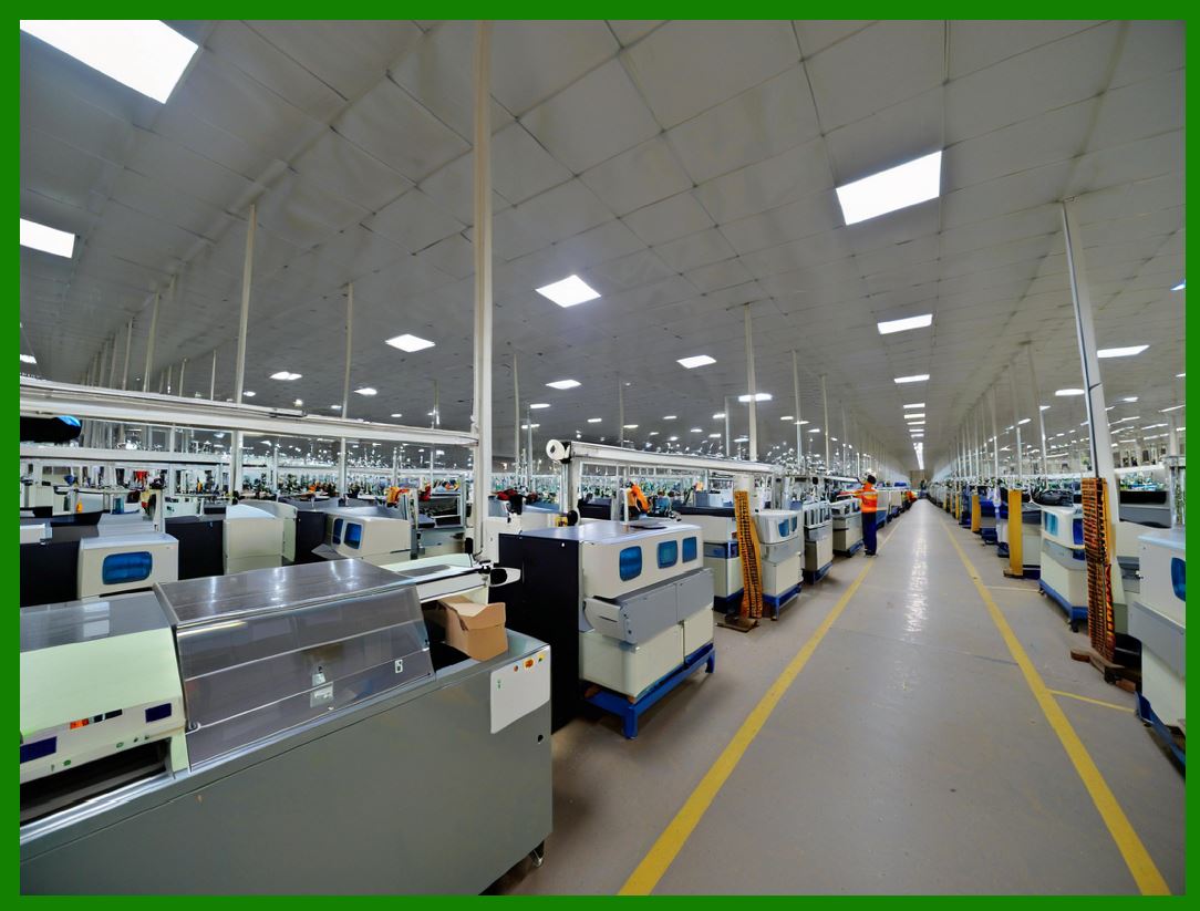
15. Manufacturing Considerations |
15.1 PCB Fabrication Constraints |
1. Controlled impedance requirements |
2. Fine-pitch component placement |
15.2 Assembly Testing Circuits |
1. Built-in self-test (BIST) circuits |
|
16. Reliability Engineering |
1. Redundant power paths |
2. Fault detection circuits |
3. Long-term stability design |
|
17. Future Circuit Design Trends |
17.1 System-on-Chip Integration |
1. More functions integrated into single silicon |
17.2 AI Accelerator Circuits |
1. Dedicated neural processing hardware |
17.3 Ultra-Low Power Circuits |
1. Designed for IoT scanning devices |

|
18. Summary of Part 17 |
1. Circuit-level design is the foundation of scanner functionality. |
2. It integrates power, sensor, processing, memory, and communication systems. |
3. High-speed signal integrity and noise control are critical. |
4. Modern scanners use highly integrated mixed-signal PCB architectures. |
5. Future designs will move toward full system-on-chip integration and AI acceleration. |

|
Next Step |
Part 18: Advanced Signal Processing Pipelines and Image Reconstruction Techniques in Image-Based Scanners |
 cs@easiersoft.com