DataMatrix Decoded: A Technical Deep-Dive |
Executive Summary |
In the semiconductor industry, where individual chips are measured in millimeters and manufacturing processes involve hundreds of intricate steps, traceability is not a luxury---it is an absolute necessity. DataMatrix codes have become the foundational technology for identifying and tracking semiconductor wafers, individual dies, and packaged components throughout the entire manufacturing lifecycle. These tiny, permanent marks link each physical unit to a digital history of electrical test data, yield analysis, binning information, and process parameters. |
The application of DataMatrix in semiconductor manufacturing is governed by rigorous industry standards, particularly from Semiconductor Equipment and Materials International (SEMI). The SEMI T7 specification mandates laser-scribed DataMatrix symbols on the back surface of double-side polished wafers, with specific dimensions and format requirements . For lead frames and strip-level traceability, SEMI T9 defines the use of 2D DataMatrix codes that enable die-level tracking from wafer fabrication through packaging and test . |
This article explores the technical foundations of DataMatrix marking in semiconductor manufacturing, the standards and technologies that make it work, and real-world applications that demonstrate how this tiny code enables the massive, complex production of the world's most critical electronic devices. |

|
Part One: The Technical Foundations of Semiconductor Traceability |
Chapter 1: Why Traceability Matters in Semiconductors |
Semiconductor manufacturing is one of the most complex industrial processes ever devised. A single advanced chip can involve over a thousand individual process steps across multiple facilities and even multiple countries. Identifying the source of a defect that reduces yield or causes a field failure requires the ability to trace a specific die back to its original wafer, the production tool that processed it, the batch of materials used, and the specific process conditions . |
Without traceability, a single defect could lead to massive scrap, extended production delays, or undetected quality issues reaching the market. With traceability, manufacturers can quickly isolate the root cause of a problem, contain affected product, and implement corrective actions. This is why the semiconductor industry has invested heavily in DataMatrix-based traceability systems. |

|
Chapter 2: The SEMI Standards Framework |
The semiconductor industry's traceability efforts are coordinated through SEMI, the global industry association that develops standards for semiconductor manufacturing. Several SEMI standards relate to DataMatrix marking: |
- SEMI T7 specifies DataMatrix code symbols on the back surface of double-side polished silicon wafers |
- SEMI T9 defines DataMatrix codes for lead frames used in packaging |
- SEMI T3 covers wafer box labels that incorporate DataMatrix symbols for container-level traceability |
- SEMI M45 relates to 300mm wafer shipping systems and includes label requirements |
These standards ensure that DataMatrix symbols applied by different suppliers and at different manufacturing stages can be read by common equipment throughout the fab. |

|
Chapter 3: The DataMatrix Symbol Specifications for Wafers |
The SEMI T7 standard specifies a specific DataMatrix format for wafer marking: an 8-row by 32-column rectangular DataMatrix symbol, with total dimensions of approximately 1.0 millimeter by 4.0 millimeters . The symbol encodes the wafer ID (an 8-character vendor-assigned identifier) and a 2-character vendor ID, with two SEMI M13 check characters automatically appended for error detection . |
Laser scribing is the mandated marking technology for SEMI T7 compliance . This ensures the mark is permanent, high-contrast, and capable of surviving subsequent processing steps. |
Chapter 4: Marking Technologies for Semiconductor Components |
The semiconductor industry uses several marking technologies to apply DataMatrix codes, each suited to different materials and stages of the manufacturing process: |

|
Chapter 5: Laser Etching for Wafers |
Laser etching is the primary method for marking DataMatrix codes on silicon wafers. The SEMI T7 standard specifies laser scribing as the required marking method . A fiber laser or UV laser can create permanent marks on the wafer surface, typically on the backside of the wafer (the side opposite the active circuitry) to avoid interfering with chip functionality. |
Early experiments with DataMatrix marking on reticles demonstrated that codes with pixel sizes as small as 0.10 millimeters could be reliably read, with the technology proving capable of decoding even when as many as 40 pixels were misread . |
Chapter 6: Dot Peen Marking for Packages and Lead Frames |
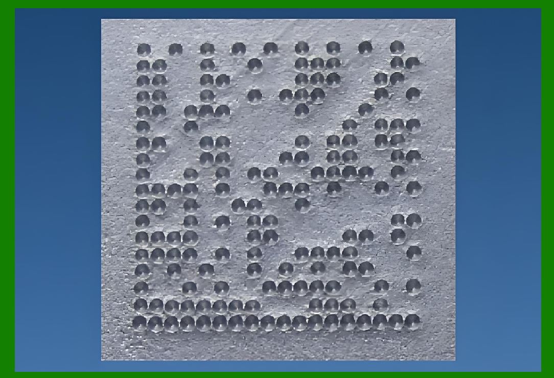
For semiconductor packages and lead frames, dot peen marking offers a robust alternative to laser etching. Systems like the Monode ICE Series provide precision marking of DataMatrix codes on a wide range of semiconductor substrates, including bare silicon dies, ceramic packages, plastic ICs, and copper lead frames . |
Dot peen marking offers several advantages: it is a mechanical process that does not introduce heat or chemical contamination, making it suitable for cleanroom environments; it creates deep, durable marks that survive aggressive cleaning and chemical exposure; and it can be applied to materials that are difficult to laser-mark . |

|
Chapter 7: Inkjet Marking |
Continuous inkjet printing was considered in early semiconductor traceability efforts as a potential marking method, with initial equipment costs around $1,500. However, the use of methyl ethyl ketone (MEK)-based inks presented safety and environmental concerns in some facilities . While inkjet remains a viable option for some applications, laser and dot peen have become the dominant technologies for semiconductor DataMatrix marking. |
Chapter 8: The Challenges of Wafer Marking |
Marking DataMatrix codes on silicon wafers presents unique challenges. Silicon is a highly reflective material, making contrast difficult to achieve with conventional imaging. The DOE/NASA study on DataMatrix for reticle identification found that even with contrast as low as 10%, DataMatrix codes were readable . This low-contrast tolerance is critical for semiconductor applications. |
To address reflectivity challenges, specialized illumination techniques are required. Red or infrared illumination can improve contrast, with infrared capable of penetrating certain surface coatings . For double-side polished wafers, marks may need to be read through the substrate, which can introduce interference signatures but does not compromise readability when using DataMatrix . |
|
Chapter 9: The 2x2 Millimeter Code Standard for Lead Frames |
For lead frames in strip packaging, the SEMI T9 standard specifies Data Matrix symbols with a cell size of 100 micrometers. The mark typically encodes a 22-character strip ID . This compact code enables traceability at the individual strip level, which is then used to track the hundreds or thousands of dies that will be processed on that strip. |
Chapter 10: Mark, Verify, Read, Communicate |
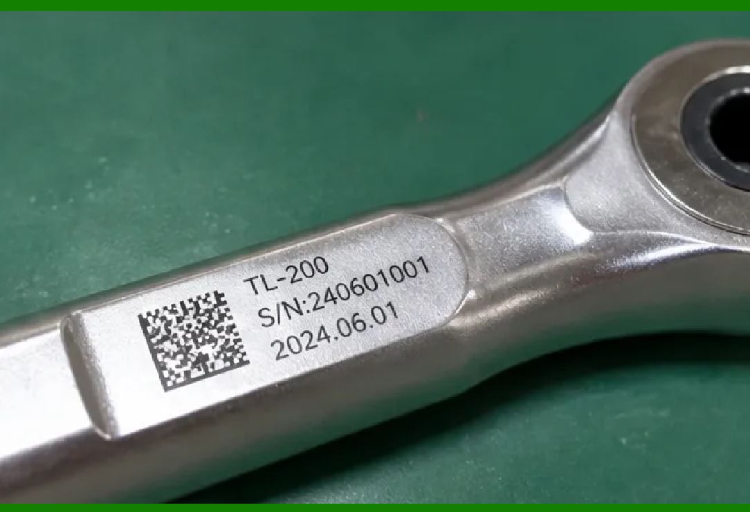
The system-level methodology for implementing unit-level traceability in semiconductor manufacturing is often described as 'Mark, Verify, Read, Communicate' (MVRC) . Marking is the application of the DataMatrix code, verification ensures the mark meets quality standards, reading captures the data at subsequent process steps, and communication transfers the data between manufacturing systems. |
|
Part Two: The DataMatrix Ecosystem for Semiconductor Traceability |
Chapter 11: Wafer ID and the Digital Map |
The DataMatrix code on a wafer encodes a unique wafer ID. This ID is conceptually similar to a driver's license number---it uniquely identifies that specific item . But the ID alone is only one half of the traceability equation. The second half is the 'map' that resides in a computer database and associates the ID with additional data: the wafer's manufacturing history, the locations of individual dies on the wafer, test results, and binning information . |
Chapter 12: Strip Maps for Packaging |
For strip packaging, a strip ID (also encoded in a DataMatrix code) enables tracking of dies through packaging and test. When a strip enters a piece of equipment, the strip ID is read, and the equipment requests the strip map associated with that ID from the factory computer. The strip map contains information about where good dies are located on the strip, enabling the equipment to focus processing on valid sites . |

|
Chapter 13: Wafer Maps in WLP and Packaging |
Wafer maps are widely used between wafer test and die attach to transfer good die locations. In wafer-level packaging (WLP), these maps guide inspection processes so that only electrically good dies are inspected. If a die fails inspection, the wafer map is updated, and the updated map is available to the next piece of equipment in the manufacturing flow . |
Chapter 14: Linking Wafer ID to Strip ID |
The link between wafer ID and strip ID is established at die attach. The equipment uses the wafer map to identify which dies are known good. It picks those dies and places them onto a strip. A new strip map is generated at die attach and uploaded to the factory computer, establishing the link: this specific strip now contains dies that came from this specific wafer. This linkage enables traceability from final test back to wafer fabrication . |

|
Chapter 15: DataMatrix for Individual Dies |
The ultimate goal of semiconductor traceability is die-level identification---the ability to trace an individual packaged chip back to its specific location on a specific wafer. This requires marking DataMatrix codes either on individual dies or, more commonly, on the strip or substrate that holds the dies, with the equipment tracking which die is at which location . |
Chapter 16: Miniature Identifier Chips |
An emerging approach for die-level traceability involves miniature identifier chips that are placed onto the substrate like any other component. These tiny chips, each containing a high-density DataMatrix code, provide a unique identifier for each die or for groups of dies. The codes can be read by automated vision systems, enabling traceability at the individual unit level . |

|
Chapter 17: Automated Reticle Identification |
DataMatrix technology has also been applied to photomasks (reticles) used in wafer lithography. A study for the 19th Annual Symposium on Photomask Technology demonstrated that DataMatrix marks on reticles could be read reliably through transparent and semi-transparent carriers, with marks on both the chrome side and the glass side readable. The study concluded that DataMatrix was an excellent candidate for automated reticle identification . |

|
Part Three: American Applications in Semiconductor Manufacturing |
Chapter 18: Cognex In-Sight Wafer Reader Series - Overcoming Illumination Challenges |
Cognex, a leading American provider of machine vision systems, developed the In-Sight 1720 series of wafer readers specifically to address the challenges of reading DataMatrix codes on silicon wafers. The series includes three models: the 1720 with a 752 by 480 pixel CMOS sensor, the 1721 with a high-resolution 1024 by 768 CCD sensor for 300mm wafers, and the 1722 with patented infrared illumination for reading codes on oxide, nitride, and polyimide wafer coatings . |
The infrared illumination of the In-Sight 1722 is specifically designed to penetrate thin films and coatings that would otherwise obscure the DataMatrix mark. This capability is critical for advanced semiconductor manufacturing processes where wafer surfaces are coated with various materials that can make visible-light reading challenging . |
Cognex's extensive experience is demonstrated by the fact that, as of 2007, the company had installed more than 25,000 wafer readers in semiconductor manufacturing facilities worldwide . |

|
Chapter 19: Monode Semiconductor Marking Systems - American Precision |
Monode, an American manufacturer based in the United States, produces precision marking systems specifically designed for semiconductor applications. The Monode ICE Series, a fixed-station dot peen marking system, is engineered for permanent, high-contrast identification of semiconductor components, lead frames, packages, and substrates . |
The system offers several features critical for semiconductor traceability: |
- CNC-controlled X-Y motion platform with (+-)0.02 millimeter repeatability across a 120 by 100 millimeter marking field |
- Adjustable marking force from 0.1 to 10 Newtons, optimized for different materials |
- Ethernet and Wi-Fi connectivity for integration with factory MES systems |
- Timestamped marking logs with operator ID and mark verification status |
The Monode Portable Pin Marker provides the same functionality in a compact, battery-powered handheld form factor, enabling traceability marking in cleanrooms and field locations where fixed systems would be impractical . |

|
Chapter 20: Monode Systems and Counterfeit Prevention |
In semiconductor and defense applications, DataMatrix marking serves as a critical defense against counterfeiting. The Monode ICE Series provides permanent UID marking on semiconductor packages per Department of Defense UID Policy and NATO Stock Number requirements . The marks are also compliant with MIL-STD-130 standards for UID marking, ensuring they meet military readability requirements . |
Chapter 21: DOE/NASA Reticle Marking Study |
The DOE/NASA study on DataMatrix for photomask identification conducted extensive testing of DataMatrix marks under various conditions. The study tested 44 different DataMatrix marks on reticles, with pixel sizes from 1.0 millimeter down to 0.05 millimeter. All marks were read and decoded successfully, with no read failures occurring across more than 25 reads per mark . |
Key findings from the study included: |
- DataMatrix marks on glass-side reticles were equally as readable as those on the chrome side |
- Marks could be read through transparent carrier materials, including amber-tinted plastic |
- DataMatrix decoded accurately even when as many as 40 pixels were misread |
- Marks with contrast as low as 10% were readable |
The study concluded that DataMatrix was an excellent candidate for automated reticle identification, with pixel size being largely irrelevant to readability . |

|
Chapter 22: DMC Marked Lift-out Grids for Failure Analysis |
In semiconductor failure analysis and materials science, specially designed 'lift-out grids' featuring DataMatrix codes (DMCs) are used for automated sample traceability in transmission electron microscopy (TEM) workflows. Each grid carries a unique machine-readable 2D micro-barcode etched directly onto the grid surface . |
This technology enables automated systems to track a specific specimen's 'life story'---from focused ion beam (FIB) milling to TEM imaging and long-term storage---without human data-entry errors. The DataMatrix codes are highly robust, remaining readable even if up to 30% of the code is damaged or obscured during the milling process . |
The approach is often aligned with SEMI E177 standards, which aim to unify the form factor for automated robotic handling in high-volume failure analysis . |
Chapter 23: SEMI T7 Compliance in American Fabs |
SEMI T7-0302, the Data Matrix specification for wafer back surface marking, has been approved by the Global Traceability Committee and the North American Traceability Committee . Major semiconductor manufacturers in the United States are required to mark wafers with DataMatrix symbols according to this standard, ensuring compatibility between different fabs and equipment suppliers. |

|
Chapter 24: Wafer Box Labeling for Logistics |
SEMI T3 provides specifications for wafer box labels that incorporate DataMatrix code symbols. These labels are applied in cleanroom environments concurrent with the completion of production of the wafers. The DataMatrix symbol accommodates substantially more information than traditional barcode symbols, providing for a unified traceability system across the factory . |
Chapter 25: DataMatrix as a Digital Passport |
The DataMatrix code on a semiconductor component serves as a digital passport, linking the physical part to its entire history. Technologies like 2D codes enable lifecycle tracking from wafer fabrication through packaging, assembly, test, and field deployment. This traceability is essential for quality management, recall response, counterfeit prevention, and regulatory compliance. |

|
Detailed Summary |
DataMatrix codes have become an indispensable tool for semiconductor traceability, enabling manufacturers to track individual wafers, dies, and packaged components throughout the complex global manufacturing process. The technology's compact size and low-contrast tolerance make it ideal for semiconductor applications, where markable spaces are measured in millimeters and surfaces are often reflective. |
The semiconductor industry's traceability efforts are coordinated through SEMI, with a comprehensive framework of standards: |
- SEMI T7 specifies DataMatrix codes on double-side polished wafers, with laser scribing as the mandated marking method |
- SEMI T9 defines DataMatrix codes for lead frame traceability |
- SEMI T3 covers wafer box labels with DataMatrix symbols |
These standards ensure that DataMatrix codes applied by different suppliers and at different stages can be read consistently. |
The technologies used for semiconductor DataMatrix marking include laser etching, which provides permanent, high-contrast marks on silicon wafers; dot peen marking, which is used for packages and lead frames; and inkjet printing for some applications . Each technology is chosen based on material, process requirements, and durability needs. |
Real-world applications demonstrate DataMatrix's critical role. Cognex's In-Sight wafer readers, with specialized illumination including infrared for coated wafers, have been installed more than 25,000 times in semiconductor facilities worldwide . Monode's American-made marking systems provide permanent DataMatrix identification on semiconductor packages and lead frames, with precision and durability that meet military and defense requirements . DOE/NASA studies have demonstrated DataMatrix readability under adverse conditions including low contrast (10%) and damage (up to 40 misread pixels) . DMC-marked lift-out grids enable automated traceability in TEM failure analysis workflows . |
The traceability enabled by DataMatrix is not merely a record-keeping exercise---it is the foundation for yield management, quality control, recall response, and regulatory compliance. When a defect is detected in the field, DataMatrix traceability allows manufacturers to identify exactly which die from which wafer is affected, enabling rapid containment and minimizing the scope of corrective actions. |

|
From the raw wafer to the finished chip, DataMatrix codes silently ensure that every semiconductor component is identifiable, traceable, and accountable. This tiny technology underpins the modern world's most essential devices---our smartphones, computers, cars, medical equipment, and defense systems---by ensuring that the chips inside them are built to the highest standards of quality and reliability. |
 cs@easiersoft.com