1. Introduction to Moore's Law and Its Impact on Semiconductor Progress |
Moore's Law, first articulated by Gordon Moore in 1965, predicted that the number of transistors on a microchip would double approximately every two years, leading to a corresponding increase in computational power. This observation served as a guiding principle for semiconductor development for decades, driving technological advancements in computing, consumer electronics, telecommunications, and countless other fields. Moore's Law fueled the rapid progression of the semiconductor industry, enabling the production of faster, more efficient, and smaller electronic devices. |
However, as transistors continue to shrink and approach the atomic scale, significant challenges have emerged that threaten the future of Moore's Law. These challenges are primarily due to physical and quantum mechanical limitations inherent in silicon-based transistors. While Moore's Law has been remarkably accurate for several decades, it is becoming increasingly difficult to sustain the pace of advancement predicted by Moore's original observation. |
This essay explores the physical limits of Moore's Law, focusing on quantum effects, the challenges of transistor miniaturization, and the diminishing returns from further scaling. By examining these factors in detail, we can gain a clearer understanding of the current state of semiconductor technology and the potential paths forward. |
|
2. Quantum Effects and Their Impact on Semiconductor Performance |
As transistors scale down to sizes approaching 2 nm or even 1 nm, they begin to operate at scales where quantum mechanical effects cannot be ignored. In classical physics, electrical currents flow in predictable paths, governed by the movement of electrons in conductors. However, at the scale of nanometers, electron behavior is governed by quantum mechanics, leading to a series of phenomena that can undermine the performance and efficiency of semiconductor devices. |
One of the most significant quantum mechanical effects encountered in miniaturized transistors is electron tunneling. In classical transistors, electrons flow through a gate in a predictable manner, with a clear distinction between the 'on' and 'off' states. However, as transistors shrink, the physical separation between the gate and the channel narrows. At very small scales, electrons can 'tunnel' through the insulating material that separates the gate and the channel, even when the transistor is in the 'off' state. This phenomenon results in leakage currents, where electrons flow uncontrollably between components, leading to power loss, heat generation, and performance degradation. |
The effects of electron tunneling become more pronounced as transistors approach the 2 nm scale and below. As the insulating barriers thin, the likelihood of electron tunneling increases significantly, making it increasingly difficult to maintain the high performance and low power consumption associated with traditional transistor designs. At the same time, the ability to isolate and control the flow of electrons becomes a significant challenge for semiconductor engineers. |
Another important quantum effect that impacts miniaturized transistors is quantum fluctuations. In classical transistors, the flow of current is steady and predictable, but at the nanoscale, fluctuations in the quantum state of the system can lead to unpredictable behavior. These fluctuations can cause problems with signal integrity and make it more difficult to achieve reliable, high-speed switching. Moreover, quantum fluctuations can affect the thermal stability of transistors, further complicating efforts to design efficient and scalable devices. |
|
3. Diminishing Returns from Scaling Transistors |
Historically, transistor scaling provided significant performance gains in terms of speed, power efficiency, and chip density. As transistors became smaller, more could be packed onto a chip, allowing for increased computational power without requiring a proportional increase in energy consumption or chip size. However, as we reach smaller nodes, the benefits from simply scaling transistors are diminishing, resulting in diminishing returns. |
For instance, in the early days of semiconductor development, each new node (such as the transition from 90 nm to 65 nm) brought substantial improvements in processing power and power efficiency. However, as we approach nodes like 7 nm, 5 nm, and now 3 nm, the improvements in clock speed and power consumption are less significant than they were at larger nodes. This diminishing return is primarily due to the physical limitations of transistor scaling, such as the onset of quantum effects and the increasing difficulty of achieving reliable switching at smaller scales. |
At very small nodes, transistor performance can even degrade if the focus remains solely on scaling. For example, while transistors may become faster in terms of their switching times, the leakage currents due to quantum tunneling can offset any gains in speed by wasting energy. The increased power consumption associated with these leakage currents, combined with heat dissipation challenges, makes further scaling increasingly impractical without significant architectural changes. |
Moreover, the cost of fabrication increases exponentially as node size decreases. The complexity of manufacturing smaller transistors requires more sophisticated and expensive fabrication techniques, including extreme ultraviolet (EUV) lithography. These advanced processes come with substantial capital and operational costs, further limiting the ability to sustain the rapid progress that Moore's Law once predicted. |
|
4. The Limits of Silicon-Based Transistors |
While Moore's Law has largely been based on the continuous scaling of silicon-based transistors, silicon itself is not exempt from physical limitations. As transistor sizes shrink, the properties of silicon begin to behave in ways that undermine the performance of the semiconductor. |
One of the most pressing issues with silicon is its limited electron mobility. As transistors become smaller, the need for faster switching speeds increases. However, silicon has a relatively low electron mobility compared to other materials, which means that the electrons in a silicon transistor cannot move as quickly as in other materials. This limitation makes it increasingly difficult to achieve the high performance expected from smaller devices. |
In addition, silicon transistors rely on the formation of a thin insulating oxide layer (typically silicon dioxide) to separate the gate from the channel. As the oxide layer shrinks to accommodate smaller transistors, its ability to effectively isolate the gate from the channel diminishes, leading to issues with leakage currents and control over the transistor's behavior. |
Other materials, such as gallium arsenide and graphene, have been explored as potential replacements for silicon, as they offer better electron mobility and could help overcome some of these limitations. However, these materials come with their own set of challenges, including difficulties in mass production, integration with existing silicon processes, and cost considerations. |
|
5. Heat Dissipation and Power Consumption |
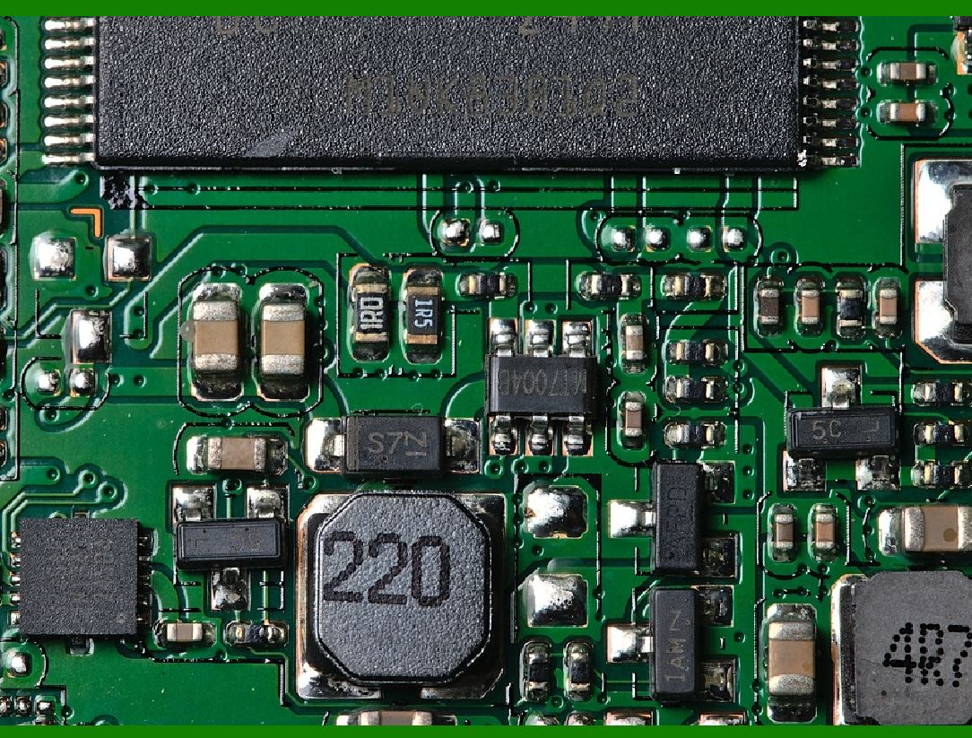
Another significant challenge to continuing Moore's Law is the issue of heat dissipation. As transistors become smaller, the power density of the chip increases, leading to higher temperatures. As more transistors are packed into a given area, the heat generated by each transistor needs to be managed efficiently to prevent overheating and ensure stable operation. |
Traditionally, the performance of a chip can be improved by increasing the clock speed, but this requires additional power. At smaller nodes, the power consumption per transistor does not decrease proportionally with scaling. In fact, at very small nodes, power consumption can actually increase due to leakage currents and the increased difficulty of controlling the transistor's behavior. |
The issue of heat dissipation becomes more problematic at the nanoscale, as it becomes harder to cool down chips effectively. The size of the transistors has become so small that traditional cooling solutions, such as heat sinks and fans, are not effective. Newer cooling technologies, such as liquid cooling or novel materials like graphene, are being explored to manage the heat generated by these high-density chips. However, these solutions add complexity, cost, and may not entirely solve the issue of heat dissipation at extreme scales. |
|
6. The Shift from Scaling to New Architectures |
Given the physical limitations of traditional silicon-based transistors, the semiconductor industry is increasingly exploring alternative architectures and new technologies to continue improving computational power. Rather than relying solely on traditional scaling, future progress is likely to come from a combination of different approaches that go beyond the simple reduction of transistor size. |
One promising direction is the development of 3D integrated circuits (ICs), where multiple layers of transistors are stacked vertically rather than being arranged on a single plane. This approach allows for greater chip density without requiring further scaling of individual transistors. By stacking transistors, manufacturers can increase the number of components on a chip without facing the same physical constraints as planar transistors. However, 3D ICs introduce new challenges in terms of heat dissipation, signal integrity, and manufacturing complexity. |
Another potential solution is the use of quantum computing. Quantum computers use qubits instead of classical bits, enabling them to process information in fundamentally different ways. While quantum computing is still in its infancy and far from being commercially viable for many practical applications, it holds the potential to solve certain types of problems exponentially faster than classical computers. This could represent a fundamental shift in the way computation is performed, potentially bypassing the limitations of classical transistor scaling altogether. |
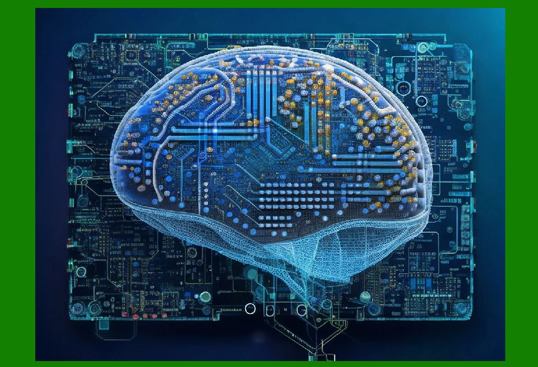
Moreover, the exploration of neuromorphic computing and artificial intelligence (AI) accelerators offers promising avenues for overcoming the limitations of Moore's Law. Neuromorphic chips, which mimic the behavior of biological neurons, can perform certain types of calculations more efficiently than traditional processors. AI accelerators, such as Google's Tensor Processing Unit (TPU) or Nvidia's graphics processing units (GPUs), are designed to perform specific tasks like machine learning more efficiently than general-purpose CPUs. |
|
7. Conclusion: The End of Traditional Moore's Law Scaling? |
The physical limits of Moore's Law are becoming increasingly apparent as transistors approach the atomic scale. Quantum effects, such as electron tunneling, are causing significant problems with leakage currents and energy efficiency, while the benefits of further transistor miniaturization are diminishing due to the onset of diminishing returns. Additionally, silicon-based transistors face fundamental material limitations that make further scaling difficult, and heat dissipation and power consumption are emerging as critical challenges in maintaining high-performance chips. |
While the traditional path of shrinking transistors may be reaching its practical limits, the semiconductor industry is not at a standstill. Instead, there is a growing focus on alternative technologies and architectures, including 3D ICs, quantum computing, and AI accelerators. These innovations may enable continued progress in computational power, even as the simple scaling of transistors becomes less effective. |
Ultimately, Moore's Law, as originally conceived, may no longer serve as the guiding principle for semiconductor development. However, the spirit of Moore's Law-continuous innovation and improvement in computational power-will likely persist, albeit through new approaches that move beyond traditional transistor scaling. |

|
What new technologies will improve this in the future? |
As traditional transistor scaling approaches its physical limits, the semiconductor industry is actively exploring a variety of new technologies and innovative approaches that could continue to drive improvements in computational power, performance, and energy efficiency. These new technologies aim to circumvent the limitations imposed by classical silicon-based scaling and quantum effects, offering new ways to process information faster, more efficiently, and at larger scales. |
Here are several key technologies and approaches that hold promise for the future of computing: |
1. 3D Integrated Circuits (3D ICs) |
3D integrated circuits (3D ICs) are one of the most promising alternatives to traditional 2D transistor scaling. Instead of continuing to shrink individual transistors, 3D ICs focus on stacking multiple layers of transistors on top of each other. This allows for more transistors to be packed into the same footprint, effectively increasing computational power without having to reduce the size of individual transistors. |
How 3D ICs help: |
Higher Density: By stacking transistors vertically, manufacturers can achieve higher transistor densities without encountering the same physical limitations as planar scaling. |
Shorter Interconnects: Shorter interconnects between stacked layers can help reduce signal delay and improve performance. |
Better Energy Efficiency: 3D ICs can reduce the power consumption associated with long interconnects between transistors, which is a major source of energy waste in traditional chips. |
However, 3D ICs come with their own challenges. Heat dissipation becomes more difficult in 3D structures, as the stacked layers trap heat more effectively than in traditional planar chips. Additionally, issues such as signal integrity, manufacturing complexity, and the need for new packaging techniques must be addressed before 3D ICs can become mainstream. |
|
2. Quantum Computing |
Quantum computing represents a fundamentally different approach to computation. Rather than relying on classical bits, which are either 0 or 1, quantum computers use qubits that can exist in multiple states simultaneously, thanks to the principles of quantum mechanics, such as superposition and entanglement. |
How Quantum Computing helps: |
Parallel Processing: Qubits can represent many possible states at once, allowing quantum computers to solve certain types of problems exponentially faster than classical computers. This makes quantum computing particularly promising for optimization, cryptography, and complex simulations. |
Exponential Speedup: For certain tasks, quantum algorithms like Shor's algorithm (for factoring large numbers) and Grover's algorithm (for searching unsorted databases) offer exponential speedup over their classical counterparts. |
However, quantum computing is still in its early stages, and many technical challenges need to be overcome, including: |
Error Correction: Quantum systems are highly sensitive to noise and interference, which can cause errors in calculations. Developing reliable error-correction schemes is a major research area. |
Scalability: Building large-scale quantum computers that can outperform classical systems on real-world problems is a significant challenge. |
Material and Cooling Requirements: Quantum computers require extremely cold temperatures and precise control of quantum states, making them difficult and expensive to scale. |
Despite these challenges, progress in quantum computing is accelerating, and in the future, it could complement classical computing, solving problems that are currently infeasible with traditional methods. |

|
3. Neuromorphic Computing |
Neuromorphic computing aims to emulate the structure and functioning of the human brain to build more efficient, cognitive computing systems. Neuromorphic chips are designed to simulate neural networks and synaptic behavior, enabling the processing of information in a way that mimics biological systems. |
How Neuromorphic Computing helps: |
Energy Efficiency: Neuromorphic systems are designed to be highly energy-efficient, similar to how the brain processes information using relatively low power. This makes them well-suited for applications in edge computing, where power consumption is a critical concern. |
Parallel Processing: Like the brain, neuromorphic systems can process multiple streams of information in parallel, making them excellent for tasks such as pattern recognition, learning, and decision-making. |
Adaptive Learning: Neuromorphic systems can adapt and rewire their connections over time, similar to the brain's ability to learn and improve performance from experience. |
Neuromorphic computing holds promise for applications like artificial intelligence (AI), robotics, and autonomous systems. However, scaling these systems to handle general-purpose computation is still a challenge, and the technology is not yet ready to replace traditional CPUs or GPUs for all tasks. |

|
4. Memristors and Resistive RAM (ReRAM) |
Memristors are a type of non-volatile memory device that stores information by changing the resistance of a material. Memristors have the potential to revolutionize memory and computing by integrating memory directly into the processing unit, allowing for faster, more efficient computation and storage. |
How Memristors help: |
Memory-Processing Integration: By combining memory and processing elements on the same chip, memristors can reduce the time and energy spent transferring data between memory and the CPU, significantly improving performance. |
Non-Volatility: Memristors retain their data even when the power is turned off, making them a more robust alternative to traditional DRAM (Dynamic Random Access Memory) and Flash memory. |
Low Power Consumption: Memristors are highly energy-efficient and could lead to ultra-low-power memory devices, which would be ideal for mobile devices, IoT applications, and data centers. |
One of the most significant applications of memristors is in ReRAM (Resistive RAM), a memory technology that uses memristors to store data. ReRAM is expected to be much faster than traditional NAND Flash and could become a key technology in the development of neuromorphic systems and future AI applications. However, challenges related to fabrication techniques and large-scale production remain. |
|
5. Carbon Nanotubes and Graphene |
Carbon nanotubes (CNTs) and graphene are advanced materials made of carbon atoms arranged in specific configurations that offer extraordinary electrical, thermal, and mechanical properties. These materials have the potential to replace silicon in transistor fabrication and solve many of the problems associated with silicon scaling. |
How Carbon Nanotubes and Graphene help: |
Higher Electron Mobility: Carbon nanotubes and graphene offer much higher electron mobility than silicon, which means they can enable faster transistors with lower energy consumption. This could help overcome some of the limitations of silicon transistors, especially as we approach the limits of Moore's Law. |
Smaller Transistor Sizes: Carbon nanotubes can be used to create much smaller transistors than silicon, enabling further scaling of semiconductor devices without encountering the same problems with electron tunneling and leakage currents. |
Thermal Conductivity: Graphene has excellent thermal conductivity, which could help with heat dissipation in dense, high-performance chips. |
Despite these advantages, there are significant technical hurdles to overcome. For example, fabricating high-quality carbon nanotubes and graphene at large scales is still challenging, and integrating these materials with existing silicon-based manufacturing processes is non-trivial. However, research in this area is ongoing, and breakthroughs could make these materials viable for mainstream semiconductor manufacturing in the coming decades. |
|
6. Photonic Computing |
Photonic computing involves using light (photons) rather than electricity (electrons) to carry and process information. Photonic devices can be much faster and more energy-efficient than electronic counterparts because photons travel faster and generate less heat than electrons. |
How Photonic Computing helps: |
High-Speed Processing: Photons can travel at the speed of light and can carry more information than electrons, enabling faster computation. |
Low Power Consumption: Photonic circuits generate much less heat than electronic circuits, which reduces the need for power-hungry cooling systems. |
Bandwidth Expansion: Photons can carry significantly more data than electrical signals, allowing for much larger bandwidths and faster data transfer rates. |
Photonic computing is still in its infancy, with challenges such as integrating photonic components with electronic systems, improving photonic circuit fabrication, and developing effective photonic memory systems. However, significant progress is being made, particularly in the realm of optical interconnects for data centers, where photonics can drastically improve data transfer rates and power efficiency. |

|
7. AI-Driven Chip Design and Automation |
Artificial intelligence (AI) and machine learning (ML) are increasingly being used to design and optimize chips. Using AI to automate the design process could lead to chips that are more efficient, faster, and better suited to specific applications. |
How AI-Driven Chip Design helps: |
Optimization: AI algorithms can be used to optimize circuit layouts, improve power efficiency, and fine-tune transistor designs at a scale and precision that would be impossible for human engineers alone. |
Custom Chip Design: AI can help design custom chips tailored for specific applications, such as AI acceleration or specialized processing tasks, enabling more efficient computation for emerging workloads. |
Faster Prototyping: AI tools can automate parts of the chip design process, reducing time-to-market for new chips and allowing engineers to focus on higher-level design challenges. |
Companies like Google, Intel, and IBM are already using AI and ML in chip design, and as these techniques improve, we can expect more sophisticated and efficient chips tailored to a wide range of applications. |
|
Conclusion: A Hybrid Future |
While the end of traditional Moore's Law scaling is drawing near, the future of semiconductor technology is likely to be a hybrid of different innovations. As traditional transistors reach their physical limits, the combination of 3D ICs, quantum computing, neuromorphic computing, memristors, carbon nanotubes, photonic computing, and AI-driven design will provide the foundation for the next wave of computing power. |
The challenge will not only be to innovate with these new technologies but also to integrate them seamlessly with existing systems and workflows. The path forward will require a multidisciplinary approach, combining materials science, electrical engineering, quantum mechanics, and AI, among others. If these emerging technologies live up to their potential, they could lead to dramatic improvements in performance, energy efficiency, and scalability for computing systems in the future. |
 cs@easiersoft.com