1. Introduction to Semiconductors |
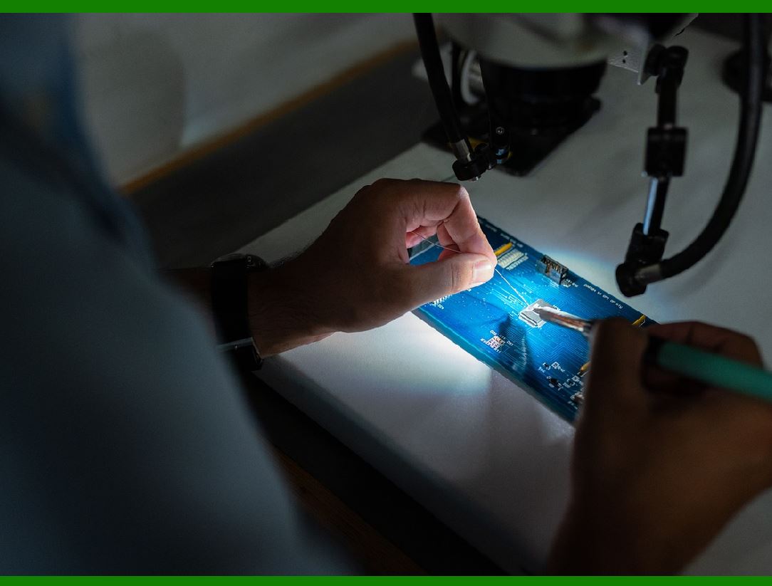
A semiconductor is a material that has electrical properties between those of a conductor (such as copper) and an insulator (like rubber or wood). This means semiconductors are not as good at conducting electricity as conductors, but they are better than insulators. This intermediate conductivity is what makes semiconductors essential for modern electronic devices. Semiconductors are the backbone of most electronic components such as transistors, diodes, integrated circuits (ICs), and solar cells. |
What sets semiconductors apart is their ability to control the flow of electrical current. This can be achieved by introducing impurities (a process called 'doping') into the material or by applying external fields, which is essential for controlling devices such as computer chips or mobile phones. The ability to switch between conductive and non-conductive states, as well as to control the flow of electricity precisely, is what allows semiconductors to serve as the basis for nearly all modern electronics. |
|
2. Properties of Semiconductors |
Semiconductors exhibit unique electrical properties that enable them to be widely used in various applications. These properties depend on both the material itself and its environment. |
2.1. Band Structure |
The electrical properties of semiconductors are often described in terms of their energy band structure. In simple terms, materials have a series of energy bands: the valence band and the conduction band. |
Valence Band: This is the highest energy band that is filled with electrons at absolute zero temperature. |
Conduction Band: This is the band that is usually empty but can be occupied by electrons when they gain enough energy. |
In a semiconductor, the gap between the valence band and the conduction band is called the bandgap. The size of this bandgap is crucial to the semiconductor's properties. In general, a semiconductor's bandgap is smaller than that of insulators, which is why semiconductors can be easily manipulated by applying external energy. |
The electrical conductivity of a semiconductor depends on the ability of electrons to move from the valence band to the conduction band, which typically requires a small amount of energy (in the form of heat, light, or an electric field). This is in contrast to conductors, where electrons are free to move even at low temperatures. |
2.2. Electrical Conductivity |
At room temperature, pure semiconductors do not conduct electricity as well as metals. However, their electrical conductivity can be significantly altered through the process of doping. When impurities are intentionally introduced into the semiconductor material, it alters the number of charge carriers (electrons or holes) available for conduction. This results in materials with n-type or p-type conductivity. |
N-type Semiconductor: When the semiconductor is doped with an element that has more valence electrons than the base material (such as doping silicon with phosphorus), it introduces extra electrons into the material, making electrons the primary charge carriers. The 'n' in n-type refers to 'negative' because electrons carry a negative charge. |
P-type Semiconductor: Conversely, when the semiconductor is doped with an element that has fewer valence electrons than the base material (such as doping silicon with boron), it creates 'holes' or vacancies where electrons can be. These holes act as positive charge carriers, hence the name 'p-type' for positive. |
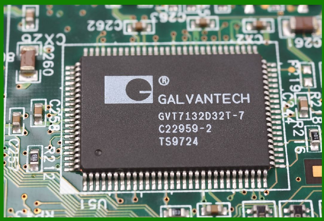
The combination of n-type and p-type semiconductors is the basis for the creation of electronic devices like diodes, transistors, and solar cells. |
|
3. Types of Semiconductors |
While the most commonly known semiconductor material is silicon (Si), other materials can also exhibit semiconductor properties. These materials can be broadly classified into two categories based on their origin: |
3.1. Intrinsic Semiconductors |
An intrinsic semiconductor is a pure semiconductor material without any significant impurities. Silicon is the most commonly used intrinsic semiconductor. In intrinsic semiconductors, the number of electrons in the conduction band equals the number of holes in the valence band. The electrical conductivity of intrinsic semiconductors depends on temperature and other environmental factors. At higher temperatures, more electrons have enough energy to jump from the valence band to the conduction band, increasing conductivity. |
3.2. Extrinsic Semiconductors |
An extrinsic semiconductor is one that has been intentionally doped with impurities to modify its electrical properties. The two primary types of extrinsic semiconductors are: |
N-type Semiconductors: As discussed earlier, these semiconductors are doped with materials that have extra electrons, such as phosphorus in silicon. This provides an abundance of negatively charged carriers (electrons) in the material. |
P-type Semiconductors: These semiconductors are doped with materials that have fewer electrons, such as boron in silicon. This creates positively charged 'holes' that act as charge carriers. |
Extrinsic semiconductors are much more commonly used in practical applications because they have much higher conductivity compared to intrinsic semiconductors. |
|
4. Manufacturing of Semiconductors |
The process of manufacturing semiconductor devices is highly complex and involves various steps to fabricate tiny components that fit on a chip or wafer. The primary material used in semiconductor manufacturing is silicon, though other materials like gallium arsenide (GaAs) are used in specific applications, particularly in high-frequency devices. |
4.1. Crystal Growth |
The manufacturing process begins with the creation of a pure, single crystal of semiconductor material. This is typically done through the Czochralski process, where a small seed crystal is dipped into a molten bath of silicon. As the seed crystal is slowly withdrawn, it grows and forms a large, single crystal of silicon. This crystal, known as a boule, is then sliced into thin wafers using diamond-tipped saws. |
4.2. Doping and Diffusion |
Once the wafer is created, the next step is doping. This involves introducing controlled amounts of impurity atoms into the semiconductor material to adjust its electrical properties. This is often done by placing the wafers in a furnace with gases containing the dopant, which diffuses into the silicon. |
4.3. Photolithography |
Photolithography is one of the most critical steps in semiconductor manufacturing. It involves applying a light-sensitive coating called photoresist to the wafer and exposing it to ultraviolet light through a mask that defines the pattern of the electronic circuit. After exposure, the wafer is developed, and unwanted areas are etched away, leaving behind a pattern on the wafer. This process is repeated multiple times with different masks to create multiple layers of components on the chip. |
4.4. Etching and Deposition |
Once the patterns are created, the next step is etching, where the exposed areas are etched away using chemicals or gases. This is followed by deposition, where thin layers of materials (such as metals or insulators) are deposited onto the wafer. These materials are used to form the wiring and insulating layers that connect the components on the chip. |
4.5. Testing and Packaging |
After the wafer has been fully processed, it is tested to ensure that all circuits are functioning as expected. Individual chips are then packaged and tested again. The final semiconductor devices are often packaged in small plastic or ceramic casings that protect them and provide connections to external circuits. |

|
5. Applications of Semiconductors |
Semiconductors are crucial in the operation of most modern electronic devices, from everyday gadgets to advanced computing systems. The applications of semiconductors can be broadly categorized into the following areas: |
5.1. Computers and Processors |
The most prominent application of semiconductors is in microprocessors and memory chips used in computers, smartphones, and servers. The central processing unit (CPU) of a computer, which performs the main computational tasks, is typically built using semiconductor materials, particularly silicon. The transistor, the fundamental building block of most semiconductor devices, is used to switch signals on and off, enabling digital computation. |
5.2. Telecommunication Devices |
Semiconductors are used in telecommunication devices such as mobile phones, routers, and satellite equipment. They enable the transmission, reception, and processing of signals in devices that form the backbone of modern communication networks. Semiconductors are critical for wireless communication, from basic mobile phone calls to high-speed internet. |
5.3. Renewable Energy |
Semiconductors also play a key role in solar cells, which convert light energy into electrical energy. These devices often use materials such as silicon or gallium arsenide to absorb sunlight and create electron-hole pairs, which generate electricity. Solar panels made from semiconductor materials have become a major source of renewable energy. |
5.4. Automotive Industry |
In the automotive industry, semiconductors are used for a variety of functions. Modern cars contain numerous chips that manage engine control, navigation systems, safety features (such as airbags), and electric powertrains in electric vehicles (EVs). Advanced driver-assistance systems (ADAS) and autonomous vehicles heavily rely on semiconductor components. |
5.5. Medical Devices |
Semiconductors are also found in medical devices, including imaging equipment (such as MRI and X-ray machines), diagnostic tools, and even prosthetics. Their ability to process signals with precision allows for the accurate monitoring and control of medical equipment. |
|
6. Future of Semiconductors |
As technology advances, the demand for faster, more efficient, and more compact semiconductor devices continues to grow. This has led to the development of nanotechnology, quantum computing, and 3D integrated circuits to push the limits of what semiconductor materials can achieve. Emerging materials like graphene and gallium nitride (GaN) also promise to revolutionize semiconductor technology by offering faster speeds, lower energy consumption, and higher efficiency. |
In summary, semiconductors are foundational to nearly all electronic devices and are critical to the development of future technologies. Their unique ability to control electrical conductivity allows for a broad range of applications across industries, including computing, telecommunications, renewable energy, automotive, and healthcare. With advancements in material science, semiconductor technology will continue to evolve and shape the future of innovation. |

|
What new technologies will be related to it? |
1. Introduction to Emerging Semiconductor Technologies |
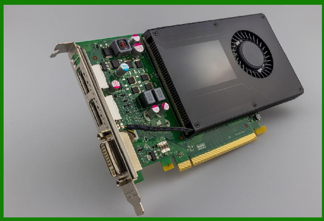
The semiconductor industry is constantly evolving as new materials, techniques, and applications are developed to meet the growing demand for faster, more efficient, and more compact electronic devices. As the limits of traditional silicon-based semiconductors approach, a wide range of new technologies are being explored to push the boundaries of what's possible. These new technologies are designed to address challenges such as heat dissipation, power efficiency, miniaturization, and speed. Below are some of the key technologies related to semiconductors that are expected to shape the future. |
|
2. Quantum Computing |
2.1. What Is Quantum Computing? |
Quantum computing is one of the most promising areas of future semiconductor technology. Unlike traditional computers, which use bits (representing either 0 or 1), quantum computers use qubits (quantum bits) that can exist in multiple states simultaneously due to quantum superposition. This enables quantum computers to process vast amounts of information in parallel, making them potentially much more powerful than classical computers for certain tasks. |
2.2. Role of Semiconductors in Quantum Computing |
Semiconductor materials, such as silicon and superconducting materials, play a crucial role in the development of quantum computing. For instance, silicon qubits have shown promise for being more scalable and easier to manufacture with existing semiconductor techniques. Researchers are developing specialized semiconductor-based devices like quantum dots (nanoscale semiconductor structures) and Josephson junctions (used in superconducting qubits) to store and manipulate quantum information. |
2.3. Challenges and Opportunities |
The primary challenge in quantum computing lies in controlling qubits and reducing quantum decoherence (the loss of quantum information due to environmental interference). However, the potential benefits of quantum computing, such as solving complex optimization problems, simulating molecular structures for drug discovery, or breaking encryption algorithms, could revolutionize industries ranging from medicine to cybersecurity. |
|
3. 3D Integrated Circuits (3D ICs) |
3.1. What Are 3D Integrated Circuits? |
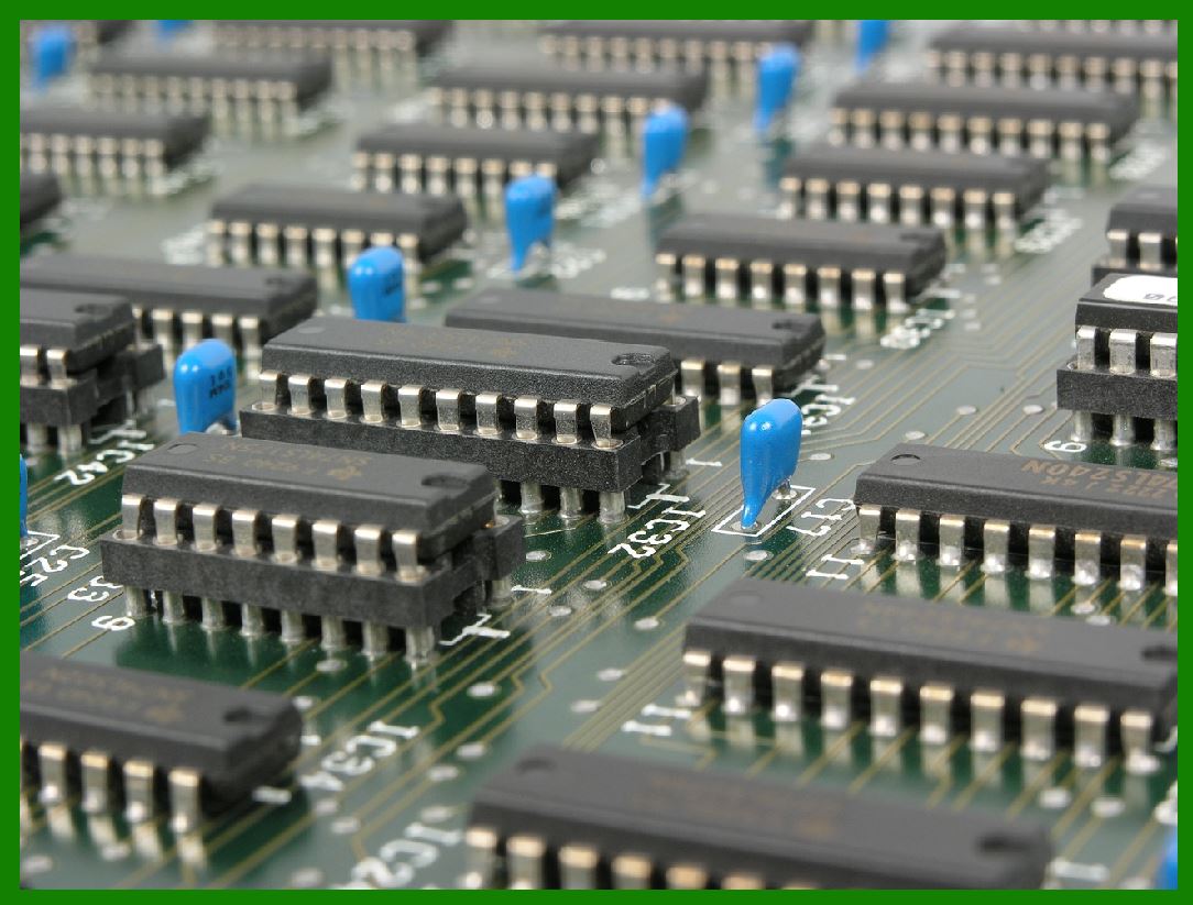
3D integrated circuits (3D ICs) are a new approach to semiconductor design that stack multiple layers of silicon wafers or chips to create a three-dimensional structure. This technology allows for much higher integration density, meaning more components can be packed into the same physical area. In a traditional 2D IC, the components are laid out in a single plane. However, in 3D ICs, individual chip layers are vertically stacked and interconnected using through-silicon vias (TSVs) or microbumps. |
3.2. Advantages of 3D ICs |
Higher Performance: By stacking chips vertically, 3D ICs reduce the distance between components, which allows for faster data transfer rates. |
Lower Power Consumption: The compact design of 3D ICs reduces the need for long interconnects, which can save power and improve efficiency. |
Smaller Form Factor: 3D ICs allow for more components to be placed in a smaller space, which is critical for portable devices like smartphones, wearables, and IoT devices. |
3.3. Challenges and Development |
Despite their potential, 3D ICs present significant challenges, including issues related to heat dissipation, manufacturing complexity, and yield (the percentage of usable chips from a batch). However, as fabrication techniques improve, 3D ICs are expected to become more viable and widely adopted in high-performance computing applications. |
|
4. Advanced Materials for Semiconductors |
4.1. Graphene |
Graphene is a single layer of carbon atoms arranged in a two-dimensional lattice. It has exceptional electrical, thermal, and mechanical properties that make it a potential candidate for next-generation semiconductor devices. Graphene is incredibly conductive, flexible, and transparent, and it could be used to create faster transistors that consume less power than those made from silicon. |
4.2. Gallium Nitride (GaN) |
Gallium nitride (GaN) is a wide-bandgap semiconductor material that has gained attention for its ability to operate at higher voltages, frequencies, and temperatures compared to silicon. GaN transistors are already used in applications like power electronics, radio frequency (RF) amplifiers, and LED technology. In the future, GaN could be used in high-efficiency power supplies, electric vehicle chargers, and telecommunications equipment. |
4.3. Silicon Carbide (SiC) |
Silicon carbide (SiC) is another wide-bandgap semiconductor material that is particularly suitable for high-power, high-temperature, and high-frequency applications. SiC is already used in power electronics for electric vehicles and renewable energy systems. As power demands increase, SiC is expected to be integral to more energy-efficient systems, especially in electric vehicles and energy conversion technologies. |
4.4. Transition Metal Dichalcogenides (TMDs) |
Transition metal dichalcogenides (TMDs) are a class of two-dimensional materials with interesting electronic and optoelectronic properties. These materials are similar to graphene but have a bandgap, making them suitable for use in transistors and optoelectronic devices. Researchers are actively studying TMDs for use in flexible displays, sensors, and low-power transistors. |
|
5. Flexible and Wearable Electronics |
5.1. What Is Flexible Electronics? |
Flexible electronics are devices that are built on flexible substrates, allowing them to bend, stretch, and conform to various shapes. These devices often use organic semiconductors, printed electronics, or thin-film transistors (TFTs), which can be manufactured on flexible materials such as plastic, paper, or fabric. |
5.2. Role of Semiconductors in Wearables |
Semiconductors in flexible electronics are essential for enabling technologies such as wearable devices (smartwatches, health monitors), flexible displays, and smart clothing. By incorporating semiconductors into flexible devices, manufacturers can create more comfortable, lightweight, and versatile products that can be worn on the body or embedded in clothing. |
5.3. Challenges and Development |
The main challenges for flexible electronics include the durability of the materials, the efficiency of organic semiconductors, and scalability. However, advances in materials science and printing technologies are expected to make flexible electronics more common in the future. |
|
6. Neuromorphic Computing |
6.1. What Is Neuromorphic Computing? |
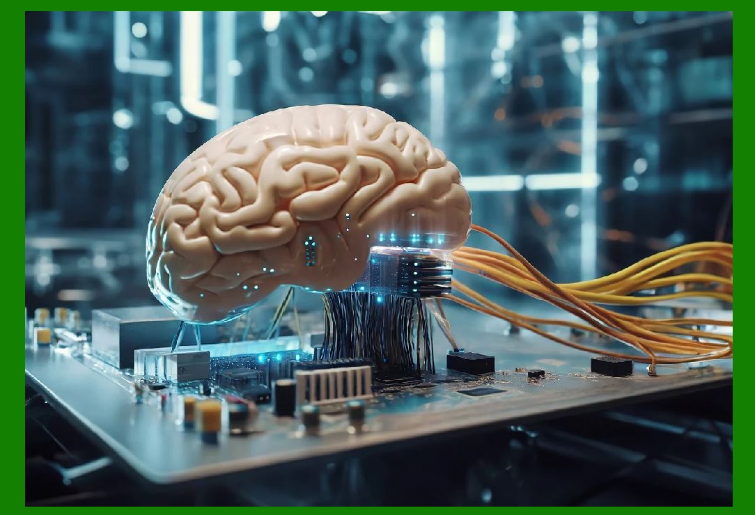
Neuromorphic computing is a branch of computing that attempts to mimic the way the human brain works. Unlike traditional computers that use binary logic (0s and 1s), neuromorphic systems use a network of artificial neurons and synapses to process information in a way that is more analogous to biological processes. |
6.2. Role of Semiconductors in Neuromorphic Systems |
Semiconductors are used to create neuromorphic chips, which are designed to emulate the electrical activity in biological neurons. These chips are expected to be more energy-efficient than traditional computers, particularly for tasks like pattern recognition, decision-making, and sensory processing. |
Neuromorphic computing has the potential to transform fields like artificial intelligence (AI), machine learning, robotics, and cognitive computing by enabling faster and more efficient processing of complex tasks. Companies like Intel and IBM have already made significant strides in developing neuromorphic chips, such as Intel's Loihi and IBM's TrueNorth. |
6.3. Challenges and Opportunities |
Building neuromorphic systems that can function efficiently at scale presents significant challenges in terms of hardware design, programming, and integration with existing computing systems. However, as AI continues to grow in importance, neuromorphic computing is expected to be a key enabler of more advanced and energy-efficient AI systems. |
|
7. Artificial Intelligence (AI) in Semiconductor Manufacturing |
7.1. AI in Design and Fabrication |
Artificial Intelligence (AI) is becoming an integral part of semiconductor manufacturing, particularly in areas like chip design, process optimization, and defect detection. AI can analyze vast amounts of data from semiconductor fabrication processes and make real-time adjustments to improve yield, reduce defects, and optimize performance. |
In chip design, AI algorithms can automate tasks like layout optimization and performance analysis, accelerating the time-to-market for new semiconductor products. AI is also being used to model new materials and simulate their behavior, helping engineers identify promising candidates for next-generation semiconductors. |
7.2. AI and Semiconductor Devices |
AI itself is also reliant on semiconductors, particularly specialized chips like graphics processing units (GPUs), tensor processing units (TPUs), and application-specific integrated circuits (ASICs), which are designed specifically for machine learning tasks. As AI technologies advance, the demand for faster and more powerful semiconductor devices will continue to grow, driving innovation in semiconductor design and manufacturing. |
|
8. Conclusion |
The future of semiconductor technology is incredibly promising, with numerous exciting developments on the horizon. From quantum computing to flexible electronics, advanced materials like graphene and GaN, and innovations in AI-driven manufacturing, semiconductors will continue to play a central role in shaping the technologies of tomorrow. As these technologies mature, they will enable more powerful, efficient, and sustainable electronic devices, revolutionizing industries such as computing, telecommunications, healthcare, and energy. The continued evolution of semiconductor technology will drive the digital transformation of the global economy and create new opportunities for innovation across various sectors. |
 cs@easiersoft.com